
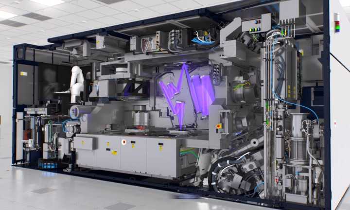
The industry can be said to gather the wisdom of almost all human science and engineering disciplines, but if you want to find a representative with the highest technological content, I think it is still a lithography machine.


The lithography process is simply two things:
1. The track component is responsible for glue spreading and development.
2. The scanner component is responsible for exposure.
It may not seem like a big deal, but in fact, it is so difficult and there are so many disciplines integrated that it may be one of the best in the development of human science.
As far as I can understand, at least it combines the wisdom of mathematics, optics, fluid mechanics, polymer physics and chemistry, surface physics and chemistry, precision instruments, machinery, automation, software, image recognition and other disciplines.
Here, let’s break down the process of the lithography process and see how it “mixes” various types of science together.
The first step is to glue.
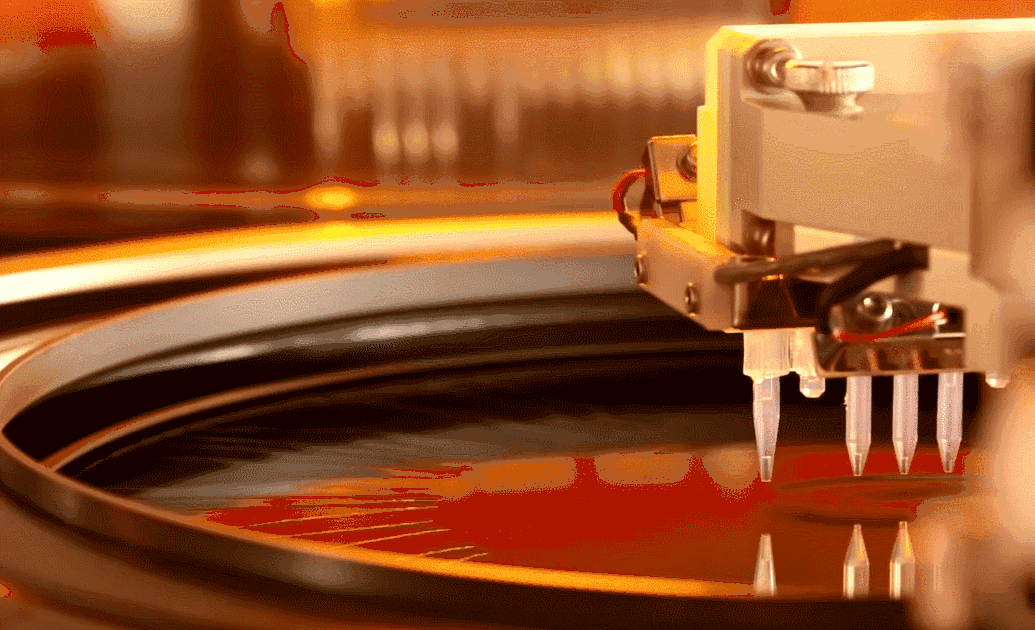

In this process, at least fluid mechanics, surface physics and chemistry are combined. The wafer is firstly hydrophobized with hexamethyldisilazane, and then the photoresist pumping system is accurately dropped in the center of the wafer. Precise volume At the same time, with the high-speed rotation of the wafer, a photoresist film with an extremely uniform thickness is finally formed (the advanced node is generally required to be within ±2nm). In this process, parameters such as hydrophobic treatment time and temperature, wafer rotation speed, photoresist dosage, concentration, and viscosity must be precisely controlled.
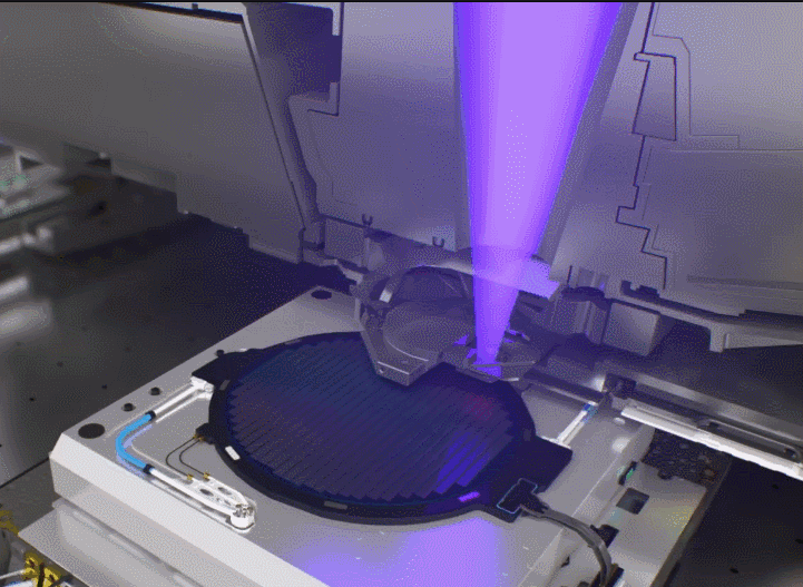
The second step is measurement and exposure.
The disciplines involved in the measurement step include at least optics and mathematics.

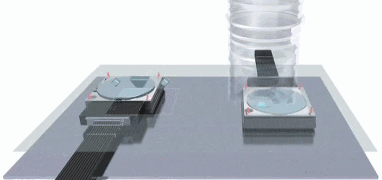
In the animation above, each wafer has undergone the process of measurement and exposure. In order to improve the output of the wafer, the wafers that have been measured (the right half of the above picture) are exposed in a step-by-step manner, and follow-up The wafer (left half of the image above) is being measured.
The main purpose of measurement is leveling, because although the photoresist has been laid very flat, its flatness cannot be regarded as a perfect plane for exposure, so it is necessary to scan and detect the entire wafer. Circular photoresist height for focus compensation during subsequent exposures.
In the process of fast scanning, the detector can quickly record and fit the leveling image of the photoresist distribution through the light feedback signal.

Exposure is a very precise process. Not to mention how precise the light source adjustment and focal length adjustment required by exposure itself are, the accuracy of wafer movement alone is amazing.

what is this concept? I converted it myself, which is equivalent to moving an object from Beijing to Shanghai (the distance is about 1000 kilometers), and the deviation between its theoretical target position and the actual arrival position is only 10 cm.
Such high-precision movements can be completed by modern lithography machines in tenths of a second.
In fact, the movement of the wafer is not so simple, because it not only has translation in the three directions of x, y, and z, but also three-dimensional rotation accompanying it to meet the best match between the focal plane and the photoresist plane, The rotation amplitude is also in the range of tens of nanometers.
So you see, just to realize the small thing of movement, it needs the coordination and unity of induction devices, mechanical devices, mathematical calculation and fitting.
The exposure process itself is more complicated. The exposure itself has extremely high requirements on the concentration of the light source and the purity of the light wavelength. The advanced process uses an excimer laser to obtain a pure light source with a shorter wavelength. This part of the content is too professional, so I will not explain it (actually because it is too complicated, and the answerer has not yet figured it out).
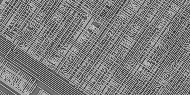
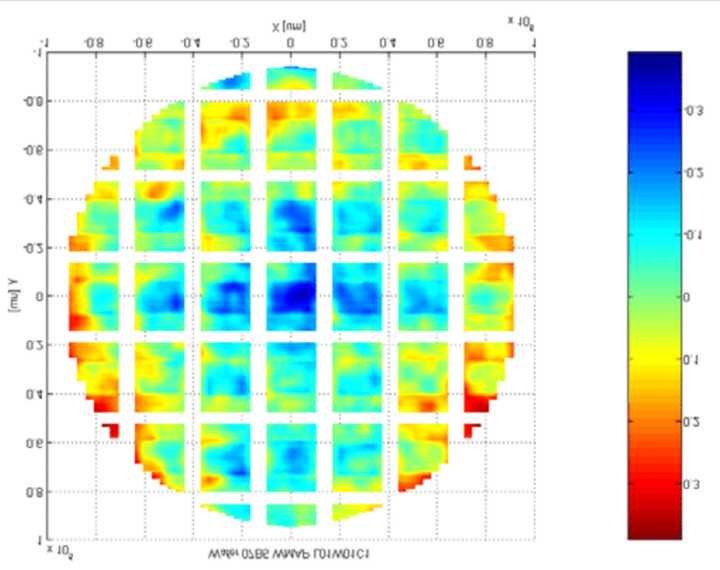
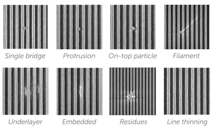
After lithography, it is necessary to evaluate the lithography effect. The most common ones are defect evaluation and critical dimension (CD) measurement.

So you see, in order to achieve a perfect lithography process, engineers have used almost all the essence of human science and engineering wisdom. From this point of view, as a representative of high-tech content in reality, I think lithography machine is well-deserved.


GIPHY App Key not set. Please check settings