Mukesh Khare, IBM vice president of hybrid cloud research, said the way to increase a chip’s performance is to increase the number of transistors, which are the core elements that process data without increasing its overall size, Engadget reported.
The 2nm chip will be able to provide 45% increased performance on devices compared to the 7nm-based chip. This means the devices will achieve the same performance as 7nm chip-powered handsets but with almost 75% less energy, according to the company.
It is also said to boost a device’s battery life by up to four times. Due to its battery life efficiency, people just have to charge their devices every four days, IBM said.
US Promises $1.2 Bn To Feed Horn Of Africa, Urges Others To Help
The 2nm chip will reportedly also increase the speed of laptops and the reaction time for autonomous vehicles. The new chip is expected to provide data centers with power efficiency that could reduce carbon footprints.
The 2nm chip will be a breakthrough in areas such as supercomputers, space exploration, artificial intelligence, as well as to 5G and 6G computing. IBM’s latest innovation has surpassed the 5nm chips that are being used by many of its competitors.
Apple’s M1 and A14 and Huawei’s Kirin 9000 use the 5nm processor. AMD and Qualcomm currently use TSMC’s 7nm processor, although the latter also uses Samsung’s 5nm chip on its Snapdragon 888. TSMC is also working on developing a 2nm chip and is planning to produce the 4nm and 3nm chips in 2022.
Because, IBM has not yet revealed when the nanochip will feature on consumer devices. Reports say it could take at least four-five years to go into production.
However, IBM, as a research institution, does not yet have the capacity for mass production, and it will take some time for 2nm process chips to go from laboratory to mass production.
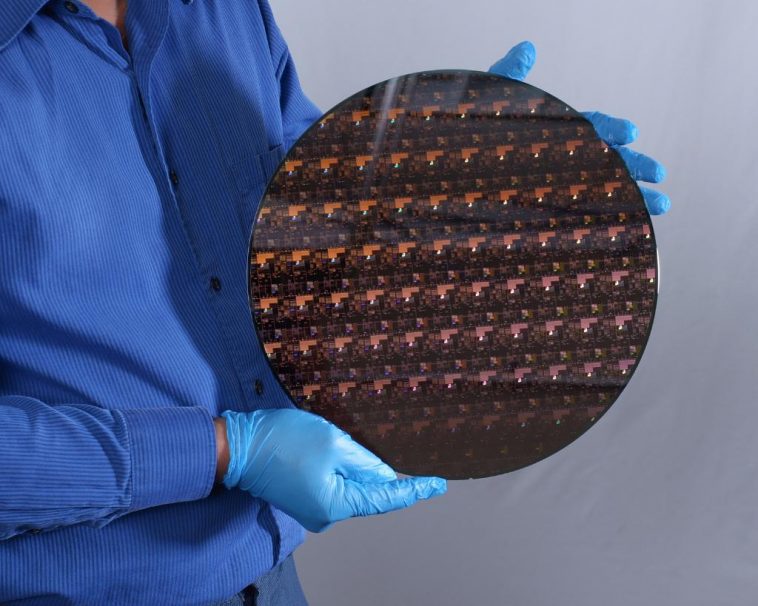
What is the concept of 2nm process? The diameter of a hair is generally 50,000 nanometers, and 2 nanometers is equivalent to 25,000 axial sections of the hair.
Previously, after announcing the successful development of a 2-nanometer chip, IBM claimed that a 2-nanometer chip the size of a fingernail could accommodate as many as 50 billion transistors. For consumers, the new technology enables the chip to reduce energy consumption by 75% and improve the performance of mobile phones, such as battery life can be extended by nearly 4 times.
However, after the 2nm process, it involves the update of the original process structure, materials, equipment, and technological innovation, which means that the industrial structure may be reshuffled, which is one of the reasons why many companies and even countries and regions decide to bet on 2nm .
In addition to the old players TSMC and Samsung, another traditional chip, according to the latest technology roadmap announced by Intel in July 2021, said that it will convert a new technical structure on its 2nm process to enhance the competitiveness of the new process. Intel has been accused of lackluster competition after the 10nm process.
Intel previously used FinFET, that is, a fin field effect transistor. The FinFET process became the mainstream process architecture of semiconductors after the 22-nanometer process and continued to 5 nanometers. Intel is about to switch to a GAAFET architecture at 2nm, full-around gate transistors, and this process architecture is seen as a successor to the FinFET process.
Samsung took the lead in introducing the GAAFET process at the 3nm node, and TSMC will also adopt the GAAFET process architecture at the 2nm node. It can be understood that the GAAFET process is the mainstream process architecture after entering the 2nm process.
Chips are also a national and regional competitive game.
According to the “Nihon Keizai Shimbun” report, Japan previously said that it will reach a consensus in the United States to establish a 2-nanometer semiconductor manufacturing base in Japan as early as 2025.
Europe, on the other hand, in its “Digital Compass 2030” planning book, put forward the goal of the development of the semiconductor industry in the next 10 years, which clearly states that by 2030, the total production value of advanced and sustainable semiconductors in Europe will account for at least the total global production. 20% of the value to overcome the 2nm process.
A new competition has begun. At present, the 2nm process is still in the research and development stage, but in the semiconductor industry with significant head effect, can the latecomers shake the status of the head enterprises?
Top circle money game
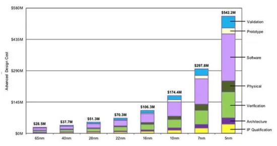
In the semiconductor manufacturing process, the 28nm process is a watershed. The process of 28nm and below is called “advanced process”, and the process above 28nm is called “mature process”. Sometimes, 28nm is also divided into the mature technology camp. 7 nanometers and below are the “high-end circle” in advanced technology. The further down the advanced manufacturing process goes, the greater the investment.
The more you go to the advanced process, the higher the complexity of EDA.


GIPHY App Key not set. Please check settings